Accelerator on a Chip

Accelerator on a Chip

wideroe_patent.png

In 1927, Rolf Wideroe pioneered the building of the first linear particle accelerators based on synchronous acceleration.  An ac signal and its inverse are alternatively directly coupled to a series of tubes in a vacuum. At the peak voltage difference particles enter the gap between the tubes and are accelerated by the electric field potential. While inside the tubes, the particles are shielded and drift. Each gap adds more energy equal to the voltage difference seen by the particles.

Linear_accelerator_animation_16frames_1.6sec.gif

This animation shows a particle emitted from source S with some initial velocity U0. Each gap adds another voltage gain. In our case, the initial velocity is 5eV and the gap potential field is +-8v or 16V. in this example our particle (either a proton or a deuteron) would have 5 + 4*16 or 69eV on exit from C4. As the particle gains velocity, each subsequent drift tube must be longer.  To accelerate a proton to 3.5Kev would require 220 stages and with a 1GHz clock would be 60.5mm long.

If the voltage is increased, fewer stages are needed to get to 3.5Kev, but the power increases with the square of the voltage. If the frequency is increased, each stage is shorter, but the power is linearly increased. In this case a 1GHz clock results in a 60.5mm long accelerator but a 2GHz clock is only 32mm long.

cb4a.JPG

To integrate a linear accelerator into a silicon chip, a 50nm wide by 50nm deep trench is etched into a dielectric layer (silicon dioxide) on a silicon wafer called the channel substrate.

cb4b.JPG

The channel wafer can be bonded to another wafer to form a closed channel. This second wafer contains the drive and control electronics and is called the logic chip. Metal patterns orthogonal to these channels are embedded in the dielectric and form the drift tube electrodes.  These electrodes are connected to the drive circuitry with through silicon vias E1 and E2.

The bonded channel substrate and the logic chip form the accelerator module. In order to sweep as large an area as possible, In order to write as wide a path as possible, 262,144 (2^18) accelerator channels are etched on a 100nm pitch. This allows at least 254,000 active accelerators per head after allowing some overlay for aligning head to head and gives an inch wide path per head. See The Print Head next.


Proton Guiding

Proton Guiding

Stolterfoht et al. (Helmholtz-Zentrum Berlin) and Ikeda et al. (Atomic Physics Laboratory, RIKEN, Japan) have been investigating the formation of charge patches on insulating capillaries that are 100nm in diameter. Protons can resonately capture a valence electron when they approach a dielectric wall such as SiO2. The proton capture time is around 1 femtosecond and the patch lifetime is around 100 seconds.

This field simulation shows 10ev protons traveling down a silicon dioxide tube lined with 0.2ev charges. The proton beams are bent away from the walls by the charges. These charge spots build up when protons are are captured and stick. The spot grows until new protons are repelled. The spot will dissipate as the protons desorb.

Field simulations of proton bending due to wall charge up

Field simulations of proton bending due to wall charge up

 
angular distribution of proton beam.png

Focus

“Transportation and focusing of accelerated proton beams by means of dielectric channels”  K A Vokhmyanina1, L A Zhilyakov2, A V Kostanovsky2, V S Kulikauskas1, V P Petukhov1 and G P Pokhil1

From the paper “Analysis of Adsorption Behavior of Cations onto Quartz Surface by Electrical Double-layer model” Kitamura, Fujiwara (1999) et. Al.  it is known that the surface charge of silicon dioxide is governed by the acid-base equilibria of silanol (SiOH) groups . The absorption of cations onto SiO2 can be analyzed using a double layer  electrostatic model as Si0-  H+. 

The paper “Local charge storage and decay mechanism in silica” by Harald Graaf*, Carsten Maedler, Christian von Borczyskowski reported that the activation energy for positive charges on the wall is 0.35eV. They demonstrate charge storage of several electron volts with the half life of the charge in the hundreds of minutes. The accumulation of these charge spots tend to focus the beam away from the walls.

 
proton density graph.JPG

Proton Injection

When protons are introduced into the accelerator from the ion injector there will be a variation in the lateral energy that will be a function of the proton temperature, proton bunching, and asymmetries in the gating electrodes. This lateral energy should be less than 1eV with a forward energy of 5eV. Protons with this little energy will either stick to the wall or tend to be deflected from charged areas on the wall.  It is expected that the initial protons in the channel will charge up the walls and that within the 50nm x 50nm channel, the beam will diverge from the walls. This provides both beam cooling and focusing towards the center of the channel.

 
tilted capillary.PNG

Exit Dispersion

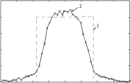
“Guiding of slow neon and molecular hydrogen ions through nanocapillaries in PET” by N. Stolterfoht et. al. 2005 shows transmission profiles for ions passing through 100nm x 10um capillaries. The walls become charged up and effectively guide the ions towards the center of the tube.

The divergence of the beam was measured as the  full width at half maximum (FWHM). where Ep is the projectile energy, qf is the final charge state of the transmitted ions, Ug is the guiding potential near the exit of the capillary. This expression is obtained from the assumption that the angle a _ vs/vp of the transmitted ions relative to the capillary axis is given by the ratio of the vertical and parallel velocities vs and vp (see Fig. 1). Moreover, it is assumed that ions with a perpendicular kinetic energy v2 s =2 larger than qfUg are lost at the surface.The divergence of the beam was measured as the  full width at half maximum (FWHM). where Ep is the projectile energy, qf is the final charge state of the transmitted ions, Ug is the guiding potential near the exit of the capillary. This expression is obtained from the assumption that the angle a _ vs/vp of the transmitted ions relative to the capillary axis is given by the ratio of the vertical and parallel velocities vs and vp (see Fig. 1). Moreover, it is assumed that ions with a perpendicular kinetic energy v2 s =2 larger than qfUg are lost at the surface.

capillary equation.PNG

This shows that the lining of the capillary prior to exit should be  conductive to avoid collecting ions on the wall that cause the exit dispersion. The beam diameter will be controlled by the beam dispersion on exit and the distance between the exit port and the wafer.

Proton Gates

Proton Gates

proton gate simulation.JPG

Proton Transistor

A proton in a vacuum channel can be controlled similar to electrons in a metal gate field effect transistor.  A low voltage (<10v) controls each channel via a metal electrode embedded in the dialectric above the channel. Protons are gated into the first cell of each accelerator channel. The first several accelerator stages bunch the protons. The pixel data is applied to the gates selecting which of the 250,000 channels write protons. These bunches of protons are accelerated as a linear array and writes on the wafer much like an inkjet printer.

Control gate off - protons pass

Control gate off - protons pass

Control gate on - protons are trapped

Control gate on - protons are trapped

 
proton gate1.JPG

Controlling the Dose

175 protons are needed to expose a 20nm pixel. Additional gate electrodes can control how full the first stage is loaded.

It is not known how important dose control will be. Since the mass of a proton is large relative to its charge, the focus of the proton bunches should stay constant regardless of the number of protons in the bunch. The length of the bunches is long relative to the diameter.

The Print Head - like an inkjet printer for protons

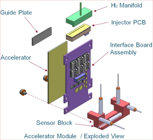
accelerator module exploded.JPG

Accelerator Module

The  accelerator chip, the ion Injector PCB, and the sensor block form the Accelerator Module. The accelerator chip is composed of the channel substrate and the logic chip. The logic chip has all the control logic that sends the write data to the proton gates. The Interface Board is a printed circuit board that has six 12-fiber connectors (total of 72 fiber data channels), power connectors, and the drift tube drive circuits. The  five Zygo ZPS laser displacement interferometers control skew, height, and adjacent head distance.

 
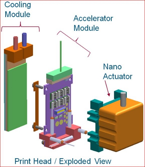
head_explode2.JPG

Print Head / Exploded

The Accelerator Module is bonded to the Cooling Module and attached to the Nano Actuator drivers. The Cooling Module bonds four Coorstek Aluminum Nitride plates that distribute and channel the coolant to keep the accelerator at a constant temperate. The temperature must be kept within 0.1 degrees centigrade to meet the CD budget. The Nano Actuator consists of piezo-electric actuators that align the head to within 2nm using feedback from the interferometers and alignment fudicials on the wafer and chuck.

 
nano actuator assembly.JPG

Nano Actuator Assembly

Surface A and B are on the same plane

Surface A is attached to Interface Board

Surface B is attached to Print Head Rail

Five Piezo actuators can move the flexure plate up/down along Z, rotate around Z, and align to neighbor.

 
print head.JPG

Print Head

The completed 20nm print head is able to write a one inch wide path on a wafer while maintaining its position in space. This means that all heads are interchangeable and do not need to be carefully installed.


print head rail.JPG

Print Head Rail Assembly

Twelve print heads attached to a ZeroDur Rail. The heads are staggered such that the back head may write the first inch of the wafer and the front head is aligned to write the next inch. The data controller compensates for the distance between the heads.


Ion Injector

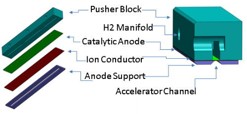
entry.PNG

The proton injector uses an anhydrous solid-state proton conductor as a cold ion source for the linear accelerator. The proton conductor is a perovskite that has a proton conduction of 1e-4 S/cm at 300 degrees kelvin.  Hydrogen enters a manifold and passes through a platinum catalytic anode. Atomic hydrogen then passes through the ion conductor where a strong electric field on the accelerator side desorbs the proton. The activation energy to remove a proton from the surface is on the order of 0.22eV.

The ion injector assembly is ~30mm by 3mm. Ions are emitted through a slit in the anode support that is 26mm by 0.3mm (300um).

 
injector_field_diagram.JPG

Ion Injector Entry Design

The active area of the ion selective membrane (ion conductor) is 2.62cm x 300um or 7.86e6 um2. Around 175 protons are required to expose a 20nm spot. Spots are written at a rate of 2e6 per second or about 3.50e8 ions/second (5.6e-11 amp) per accelerator channel. The proton current for a total array of 262,144 accelerator channels (one head) could be as much as 14.7ua.  The H+ flow rate per head is 4.1e-4 sccm.

An Eizel lens assembly extracts the ions from the ion conductive membrane and focuses them with a 30x reduction to a 15um entrance slit. This slit has a 1.43 degree bevel that leads to the proton gates.

Exposure

Accelerator Exit Port

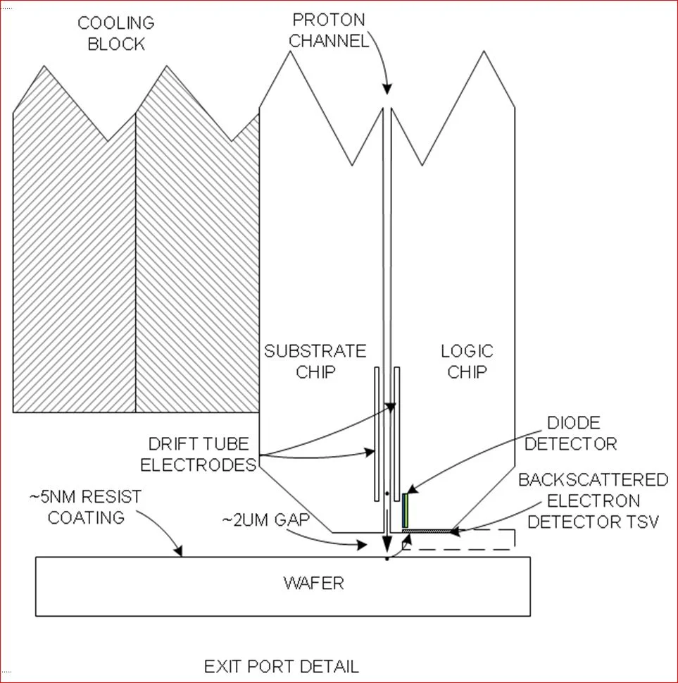
The proton beam exits the accelerator channel and travels across the head to wafer gap to expose the resist on the surface of the wafer.  Laser interferometers control the nano actuators on the print head to maintain a two micron distance to the wafer and to keep the head parallel to the surface.

Before a wafer can be exposed, the wafer topology and alignment features must be mapped and stored. Backscatter detectors embedded in the edge of the logic chip sense these features and their position is communicated to the layout controller.

exit port detail.JPG

x-y positioning.JPG

X-Y positioning

As the wafer travels under the print heads at 40cm/s a line of protons is written across the wafer every 500ns (2MHz) to produce a line of 20nm pixels.  Since the pixel is 20nm and the accelerators are on a 100nm pitch, the print heads will shift over by 20nm to paint the next row (X) of pixels. Five passes completely cover the wafer. This shifting of each print head the Y direction is done by the Nano Actuators.


exposure1.JPG

Exposure

PMMA is a popular positive resist used to achieve line widths of 4.4nm (with 50KeV electrons) (jes.ecsdl.org/content/128/1/166).  Proton beams are about 100 times more efficient than e-beams. 3.5KeV protons enter the resist moving much slower than the 50KeV electrons. Each electron only produces a few collateral electrons that are moving slow enough to split the polymer bonds. The dissociation energy for a C-C bond is 3.6eV.  The electron has to be at rest with respect to the molecule in order to react most strongly via dissociative electron attachment, where the electron comes to rest at the molecule, depositing all its kinetic energy. Protons generate on the order of 100 collateral electrons that are less than 10eV. These not only are effective in splitting the polymer bonds, they also do not spread as much as the hotter electrons from e-beams. Protons can expose PMMA with 7uC/cm2. The write energy and dose are calculated as follows:

         7e-6C/cm2 * 3500eV = 0.0245 joules/cm2

beam simulation.JPG

        7e-6C/cm2 * 6.24e18p/s = 0.437 protons/nm2

        0.437 protons/nm2 * 20nm *20nm = 175 protons per pixel


Wafer Heating

e-beam vs p-beam.JPG

The wafer absorbs the proton energy and dissipates it as heat. This will lead to some CD variation across the wafer. We can assume that 99% of the heat will be transferred to the chuck (which is cooled).

        wafer area = 3.1416 * ((.3m-.004)/2)^2 = 0.0688m2

       wafer heating @ 100% write = 0.0245 joules/cm2 * 10000 cm2/m2 * 0.688m2 = 16.9 joules

       wafer heating @ 60% write = 6.74 Joules

       wafer temperature rise = 6.74 joules * 0.01 / 37.4 joules/*C = 0.018 *C

Datapath

system data path.JPG

System Data Path

Wafer writing begins with scanning the wafer to establish alignment features and for each head to negotiate with its neighbors for track to track head alignment. The interferometers and Nano Actuators move the heads such that each head will write 254,000 100nm channels (1 inch) and that each head is perfectly aligned with its neighbor.

The mask data base is sent to the control computer. Since each channel is separately collimated, proximity correction is not necessary. The data is rasterized into 12 stripes for a 300mm wafer, one for each head. The data is repeated for each die or can be written as a whole wafer. Since there is no mask, die size limits are arbitrary.

The wafer transport system is mapped and X variation data is sent to the data controller so the write timing can be adjusted.


Data Rate Calculation

Each print head needs 62.5MB/s mask raster data to write to all of the 254K accelerators. This can easily be accomplished with 8 - 10Mb/s SerDes channels of Hybrid Memory Cube Gen 3.

The pixel data rate is computed as the binary write with no gray scale. The wafer moves in the X direction at 40mm/sec with 20nm pixels, so:

       40e-3  / 20e-9 / 8 = 2e6 writes/s

       254,000 channels * 2e6 writes/s  = 5.08e11/s per head or 62.5MB/s

The Avago MiniPOD™ AFBR-814VxyZ operates at 14.0625 Gbps for IB-FDR with 64b/66b encoded data per fiber and has 12 receivers per POD.

       5.08e11 /14e9 = 36 fibers or 3 PODs

The total data rate for all 12 heads is 0.75TB/s per station or 1.5TB/s for a twinscan configuration.

Direct Write Opens Up Many New Applications

A Different Encryption Key on Every Chip

One of the strengths of maskless lithography is the possibility of writing a different pattern to each die site. This allows for many forms of serialization and customization. Possible applications include:

  • Writing a true hardware CPU-ID onto each individual processor chip that would be impossible to change
  • Permanently storing any number of encryption keys in hardware, uniquely enabling encryption and authentication
  • Preventing counterfeiting by writing the serial number, manufacturing location and date on every chip

Secure IP

Many companies as well as government agencies must guard their intellectual property. The mask making tool chain exposes much of the underlaying design to possible theft. Maskless wafer writing can keep the design database encrypted until it the wafer is written.

Smaller Quantity ASICs

Protogype wafers could always be included with any fab run. Test features could be included or changed as needed. Mixed asic wafers such as MOSIS could be done economically and included in any fab run.

Simplified ECAD Tool Chain

Proton beam have very little interaction with each other or with wafer surface charge up, thus there is little need for proximity correction. If 193i compatibility is not needed, then less restrictive layout optimization can be done.

cryptochip.jpg